Yang Qiguo / Text
A groundbreaking wafer preparation process developed by the Tuozhong Technology Team is revolutionizing China's MEMS sensor industry. This innovation addresses the long - standing issue of over 80% dependence on imported high - end MEMS sensors, especially in strategically important areas like national defense and aerospace.
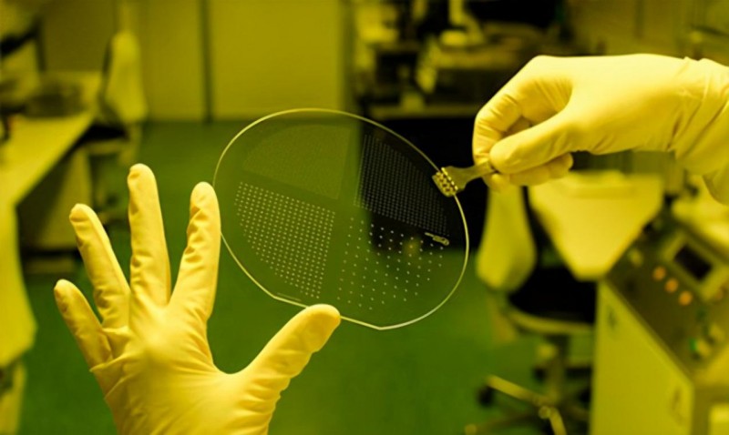
The team's three core technologies are the key to this success. The micron - level dry powder solid porous structure ensures excellent micro - scale thermal isolation, with a vacuum thermal conductivity of only 0.04W/mK. The optimized pseudo - Bosch etching process achieves an aspect ratio of 30:1 and a sidewall roughness of no more than 50nm. Additionally, the reconstructed bulk silicon MEMS long mask process significantly boosts the production capacity per batch.
This process supports both 6 - inch and 8 - inch wafer production. For 6 - inch wafers, the batch yield exceeds 95%, and each wafer can hold 576 chips, outperforming products from international giants like Bosch and Broadcom. It has been adopted in smart automotive and medical sectors, and partnerships have been established with companies including Nanjing Hongyao. Looking ahead, the team plans to expand production lines and collaborate with global firms to further advance China's sensor industry.